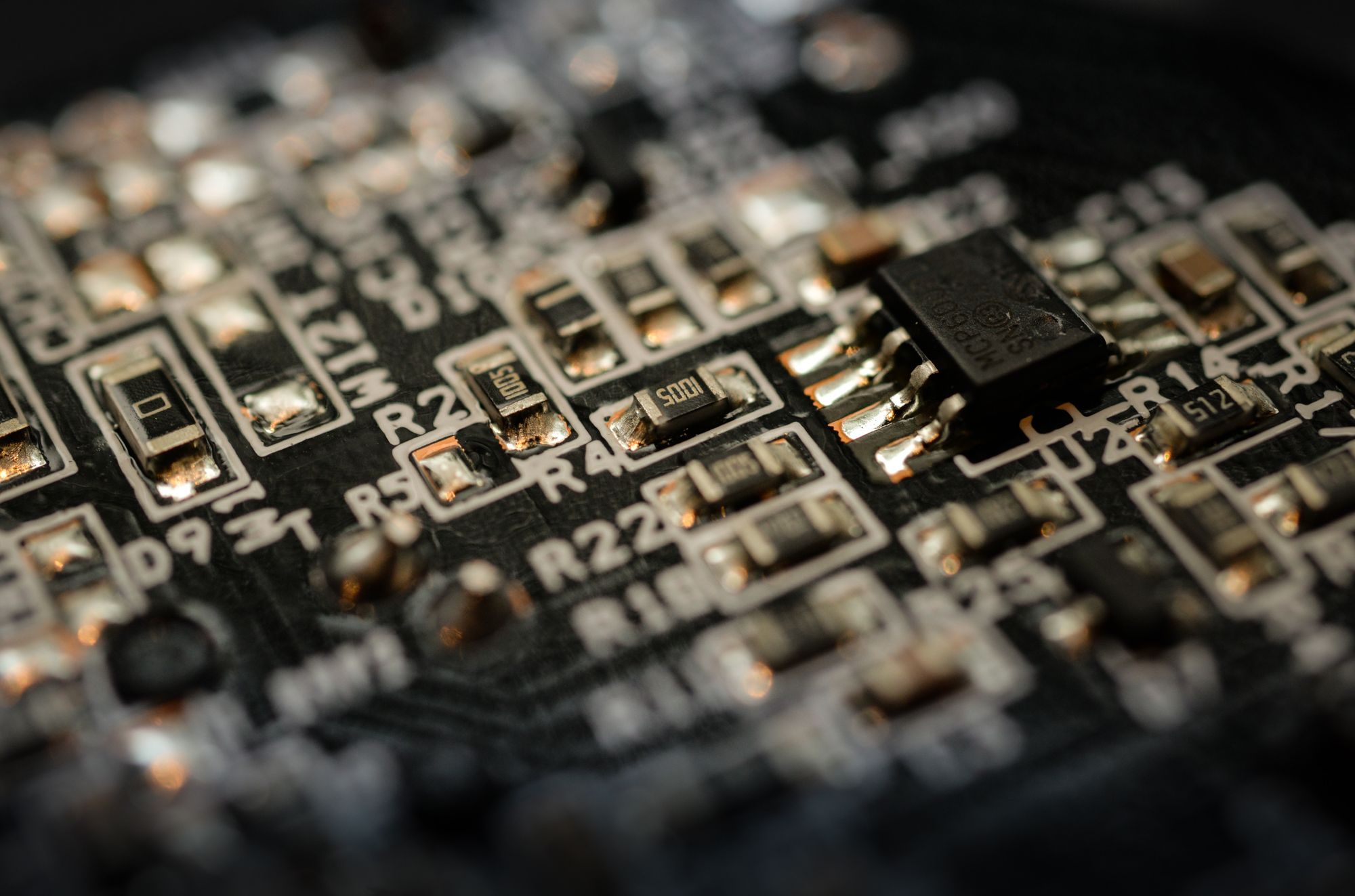
While prices for graphene have fallen dramatically over the last two decades, from hundreds of thousands of dollars per kilogram to less than $50, the price of better-quality graphene for use in electronics still remains relatively high. This is because such high-grade graphene must be free of defects, dislocations, and grain boundaries.
Engineers and product designers have understood the value that top-end graphene can provide to electrical products but can often not justify using it due to its high price.
What is badly needed is a way to produce electronics-grade graphene cheaply.
The most common way of synthesizing good-quality graphene is through chemical vapor deposition (CVD), but 2D sheeting created from this method often contain defects. If greater care is taken, and the parameters are accurately set during growing, flaws can be minimised. However, it’s a slower process which increases costs.
Alternative approaches include growth on a single-crystalline catalytic substrate, but these substrates can be expensive, again pushing up prices.
To avoid these issues, Dongmok Whang an Associate Professor at Sungkyunkwan University Advanced Institute of Nanotechnology and Jae-Hyun Lee a professor based at Ajou University and their colleagues sought an alternative method for graphene production. One that focused on speed and low cost yet could maintain high quality.
Their research found that by transferring pieces of single-crystal graphene and spacing them out on a polycrystalline substrate allowed for subsequent growing to join the pieces up. With all the transferred samples having their crystal lattices facing the same direction, the connected pieces had no grain boundaries.
The idea originated from previous research which found that the energy required to start graphene synthesis (the nucleation of new graphene seeds) is much higher that the energy required to grow graphene from the edge of a graphene seed.
“In other words,” says Lee, “it was thought that additional nucleation could be easily suppressed at lower energy conditions (e.g., low concentration of precursor or low growth temperature).”
Drawing on the team’s experience of growing large-area single-crystal monolayer graphene, the team worked on finding the best way to precision cut, transfer, and space graphene ‘seeds’.
As the scientific journal Phys.org reports, “To determine what seed size and spacing would work best, Whang and Lee and colleagues calculated the diffusion length for the temperatures and precursor concentrations used. They cut ‘seeds’ 10 μm wide from their original single-crystalline graphene sample and transferred them to polycrystalline platinum spaced 50 μm apart. Here, they grew single-crystalline graphene to cover an area of 2 cm x 2 cm.”
While the test samples have so far been small, what is important is the ability to reduce production time to a fraction of what was previously thought possible for such high-grade graphene. In addition, by using a much cheaper substrate made of polycrystalline, the team have further cut costs dramatically.
“It was difficult to grow to larger sizes due to the limitations of our CVD system,” explains Lee. “But we believe that our approach can be fully applied to large catalyst substrate.”
The study has now been published in the journal ACSNano, where they describe, “… a general approach for the scalable growth of single-crystalline graphene, which is a representative 2D material, through ‘transplanting’ uniaxially aligned graphene ‘seedlings’ onto a larger-area catalytic growth substrate.”
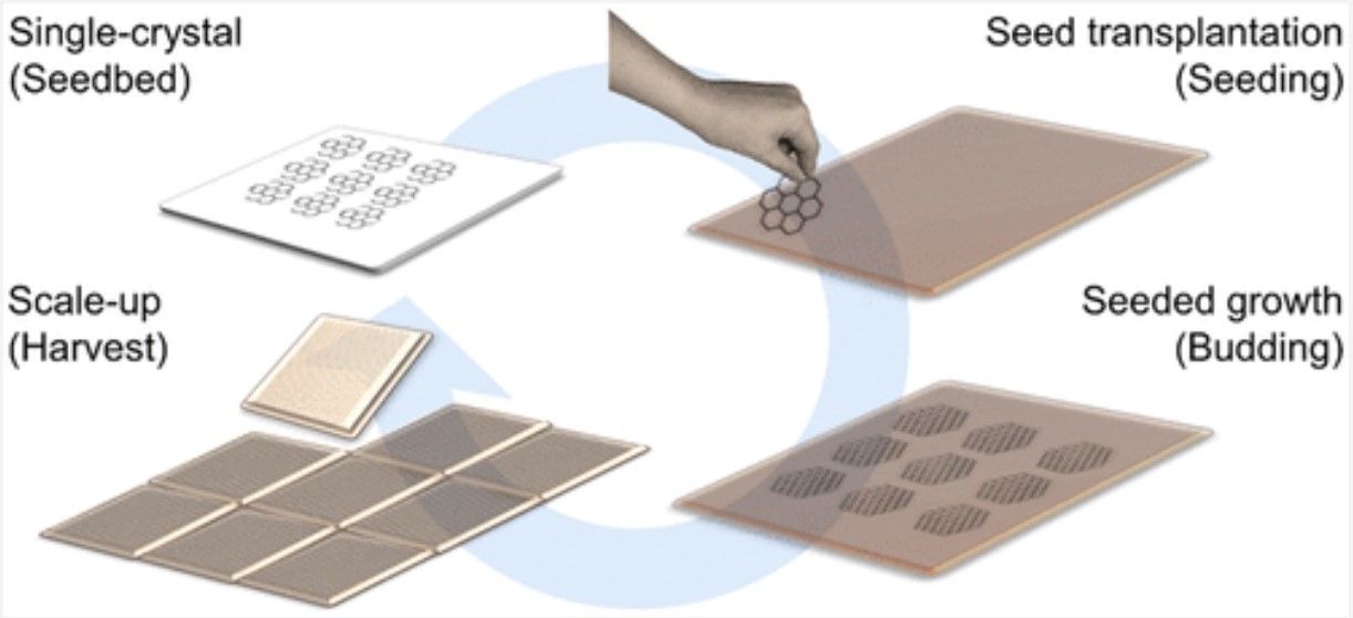
In doing so, the team, “… obtained single-crystalline graphene with an area four times larger than the mother graphene seed substrate. Moreover, the defect-healing process eliminated the inherent defects of seeds, ensuring the reliability and crystallinity of the single-crystalline graphene for industrialization.”
The end result is high-quality graphene at a lower cost than production through CVD alone.
“If the synthesis temperature, gas used, etc. are assumed to be similar,” says Lee, “the thermal budget and the price of the substrate can be said to be reduced to a quarter.”
In addition to using a cheaper polycrystalline platinum as a substrate, the team were also able to recycle the material without damaging the quality of the graphene. This further saving reduced production costs further such that, “… the resulting single-crystalline graphene … works out at around $100 dollars per cm2 of substrate instead of $2000.”
The team is now working to refine the process and expects that polycrystalline copper or even aluminium foil may work as a suitable substrate, further lowering costs. Work is also being conducted with different raw materials, to see if other 2D materials can be cut and transferred for cheaper production in a similar way, however, significant challenges remain in achieving this.
Graphene’s growth, meanwhile, is well documented and it has a simple, single carbon atom structure, adding other raw materials or combinations of substances complicates things.
“There are many variables to consider because of the different solubility and diffusion rates of each element in the catalyst,” notes Lee. “However, if we use a process that sequentially reacts one precursor and another precursor, such as an atomic layer deposition (ALD) process, which can simplify process parameters, it could be possible to grow a single crystalline monolayer of various 2-D materials.”
For now, though, the team are satisfied that their new graphene production process will have a significant impact.
History tells us how new processes for producing high-quality single-crystalline silicon wafers have lowered their price, allowing for a boom in their use in the consumer electronics market.
If the researchers are correct, making single-crystalline graphene on the cheap could pave the way for a new wave of electronic devices based on affordable nanoscale raw materials.
Photo credit: ACSNano, Photo by Skitterphoto from Pexels